A Printed Circuit Board, abbreviated as PCB is a foundation used in the design of electrical gadgets. It plays to important roles:
-
Providing mechanical support to components in the design
-
Electrically connection the components through conductive pathways
In the current electronic world, the leveraging of a PCB can result into a simple yet  compressed electronic gadget design or the creation of Very High Scale Integration designs important in the creation of microcontrollers and processing units.
PCB assembly consists of a series of intricate steps that must be followed to the latter if the product is to be of any use in the electronic design and creation fraternity.
Readying the board that will eventually be the PCB
The preparation of the board and the type of material chosen for the board varies depending on the quality of product the designer desires to achieve. The first step is in the creation of the laminate, which is achieved by pressure curing layers of cloth or paper with thermoset resin to create a final uniformly thick panel.
The type of material used in the curing determines the laminate classification hence the job it can do. Characteristics considered in classification include fire resistance, dielectric constant, loss factor, shear strength and tensile strength.
Printing the circuit into the board (etching)
This is a dynamic step whose approach varies depending on the end product desired. Most PCB assembly procedures however cover the laminate with copper on both sides and then proceed to remove the copper from unwanted places resulting into the wanted fine copper traces. This method, referred to as subtractive method, is cheap to implement but more environment polluting than the more complex additive method.
Additive PCB assemblage procedure electroplates the copper traces onto the laminate to form the desired circuitry. Though it uses less copper and creates fewer residues, it comprises of several intricate steps making it a more complex approach in comparison to the subtractive approach.
Individual approach to the etching procedure
Whatever etching approach you decide to settle for, there also are other choices to make in the implementation mode. Major approaches are
-
Large volume approach: This consists of the silkscreen printing approach, which is the main commercial approach and the photographic option used when fine line widths are needed.
-
Small volume approach: This involves printing onto a see-through film and using a
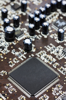 photo-mask along with photosensitized boards then etch, using laser resist ablation or using a CNC mill with a spade shaped cutter or tiny end mill to gauge off undesired copper from the laminate.
-
Hobbyist approach: This uses Laser print resistance technology that laser prints onto a transparent layer before heat transferring it with iron or bespoke laminator onto exposed laminate and then touching it up with marker before etching it. Other approaches in this category are hard to achieve in mass productions.
Drilling holes into the PCB and adding circuit components
The next step is in drilling holes through which the components in the design have to go into. This is achieved by the use of tiny diameter drill bits prepared from coated tungsten carbide. To accomplish this, you have to use high-speed automatic drills to keep away from marring and tearing up the copper tracks.
The contact ends that have to remain open are coated with a viable solder composite to ensure that the PCB will remain conductive without suffering from problems of copper oxidation.
The best way out of the mayhem
It is clear to see that PCB assembling needs heavy investment in terms of expertise and infrastructure. To avoid wasting all this money in the creation of a system that might not end up being as productive as it should be, you might have to consider the option of outsourcing. Out sourcing complete builds for use in your activities could be the simplest and cheapest way out for your enterprise.