 When you consider the RF applications utilized in mission critical C5ISR environments, your contract manufacturer (CM) must comprehend the issues and challenges related to manufacturing processes in RF, but also have a deep understanding of the failure mechanisms that can cause defects.
RF design is inherently more complex than any other type of design. This is because of the unique issues that must be addressed due to the extremely high frequencies of operation for these applications. For example, there are inherent challenges with power control, grounding structures, printed wiring board (PWB) stack-ups, laminate and surface finish selection, characteristic impedance control, signal path configurations, connectorization, pad geometries, solder mask, conformal coating, surface parasitics, exposure to harsh environments, fabrication effects, via sizing, component selection, and manufacturing process impacts. These numerous issues must be well understood by your CM or the potential for failure is magnified.
In manufacturing RF and microwave circuits everything is critical:
- Placement of die and components with respect to each other.
- Placement of wire bonds and ribbon bonds; as wire bond lengths are now inductors and part of the electrical circuit.
- Epoxy die attach: in low frequency it is not critical but in RF and Microwave epoxies must be attached immediately as resistance is crucial
- Ground is ground….attachment to the ground plane either by conductive epoxy, conductive film adhesive, or solder is extremely critical.
- For RF and microwave power amplifiers, the die attachment is critical for good thermal dissipation as well as signal integrity.
- The PCB manufacture, dielectric control, line width etc. is extremely important
- Hermetic seal and hydrogen is a concern and some companies mandate the use of a "hydrogen getter" to minimize that effect.
- Incorrect fabrication of circuit traces or plating thicknesses which impact the RF circuit functionality and typically isn't found until the assembly/test functions as it’s not possible to test functionality of the bare board.
- Contamination resulting from improper cleaning or exposure to some type of FOD/debris is also a potential issue. RF circuitry usually has covers to stop FOD/debris and for EMI control so this failure mechanism is not that common). Improper cleaning and leaving flux residue on the PWB surface is more applicable.
- Handling damage: if there is a scratch or a circuit trace gets "nicked" that can impact the RF circuit functionality, and/or performance.
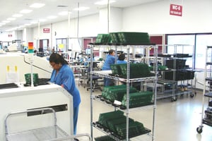
About Zentech: Zentech Manufacturing, Inc. is a privately held, engineering-driven contract manufacturer specializing in the design and manufacture of highly-complex electronic and RF circuit cards and assemblies. The company is headquartered in its purpose-built facility located in Baltimore, MD, and in Fredericksburg, VA, and maintains several key certifications, including ISO 9001:2008, ITAR (US State Dept.), AS9100 (aerospace), and ISO 13485 (medical). In addition, Zentech is a certified IPC Trusted Source supplier for Class 3 mission-critical electronics, and the company is IPC J-STD-001 Space Addendum QML certified and is now NIST 800-171 compliant. Zentech Fredericksburg operations is also a Mid-Atlantic leader in the fabrication of wire harnesses and over-molded cables for harsh environments.